Technology shapes our world in amazing new ways each day. Behind that progress are the tiny details engineers handle with care. One of those details is the wafer-an important part of electronics.
Mask design is a special step in making devices. It helps build circuits using light and patterns. But each design needs the right wafer to work well.
How can engineers get wafers that fit their exact design needs? This is where advanced custom wafer solutions come in.
These solutions support creative designs and better outcomes. Keep reading to learn how custom wafer solutions support mask design.
Understanding the Role of Wafers in Mask Design
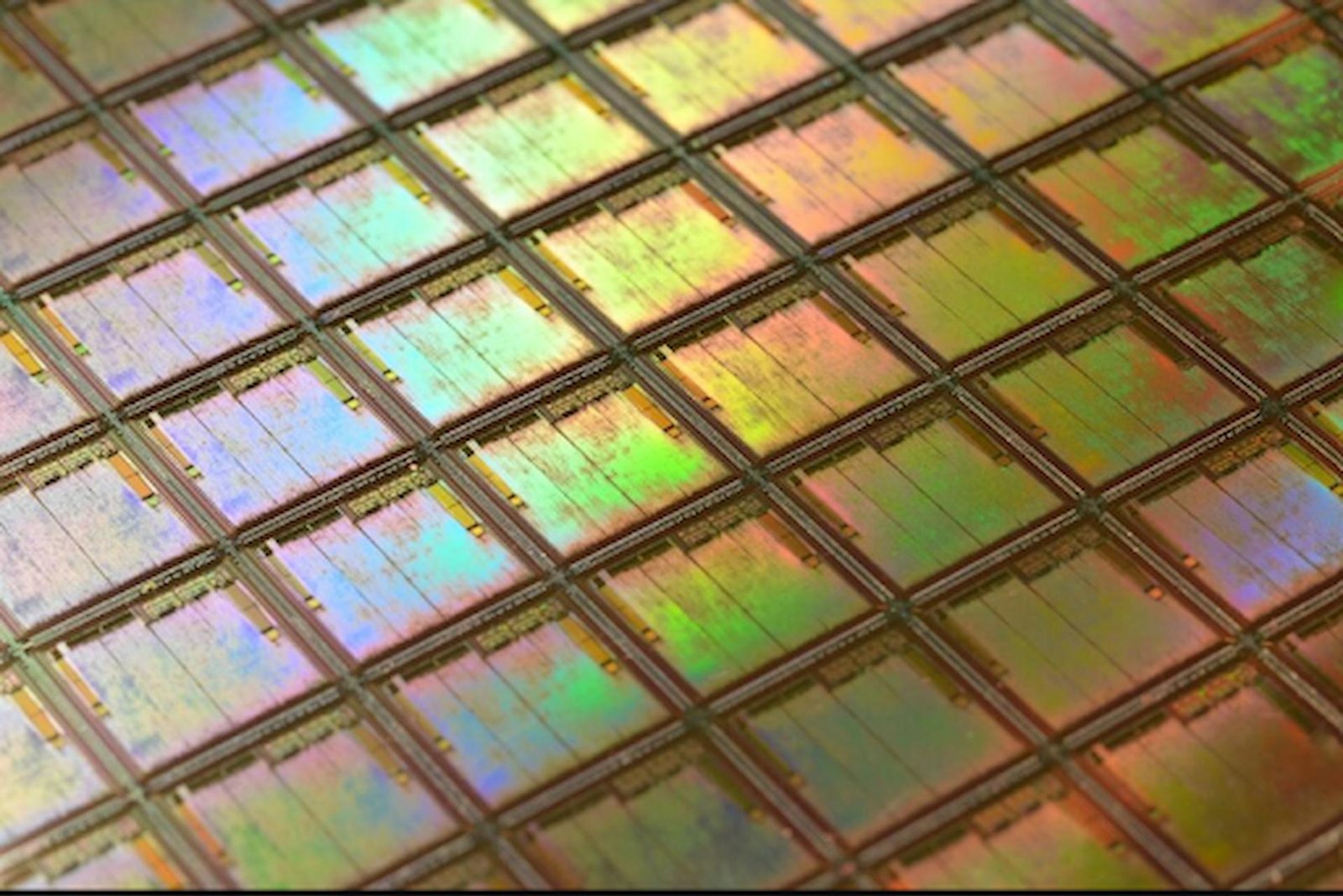
Wafers are thin slices of material used to build chips. These chips power phones, tablets, and computers. During mask design, wafers are used as a base.
A mask is like a stencil that helps shape the circuit pattern. This pattern is printed onto the wafer using special light. Every shape must match perfectly.
If the wafer doesn’t meet the design, the chip may not work. That’s why special wafers are sometimes needed. Advanced wafers are made to meet exact rules.
They help test and build chips with high accuracy. Mask design relies on clean and flat wafers.
Custom wafer solutions support this very need. They help create masks that lead to working circuits.
Why Custom Wafer Solutions Matter for Designers
Not all chip designs use the same layout or process. Some need thicker wafers. Others need different materials or shapes. That’s why custom wafer solutions are so important.
They let engineers order wafers with special features. This could mean different sizes, layers, or coatings. Custom wafers help match the mask to the exact process.
This lowers mistakes and saves both time and cost. With these solutions, designers can test better ideas. They can work faster without changing their whole setup.
Engineers can also get help with specifications and builds. Custom solutions are built with clear goals in mind. That way, the final wafer fits each mask exactly.
Key Materials Used in Custom Wafer Production
The base material of a wafer affects its performance. Silicon is the most common choice because it’s strong and reliable. But other materials like germanium or sapphire are used too.
Some designs need high heat resistance or more electrical strength. Each material helps with a different challenge. Custom wafer solutions let designers choose the right type.
They also offer options like doping or special layers. That means they can match the wafer to the mask process.
The thickness and finish of the wafer also matter. By using the best material, results are easier to predict. These choices help engineers meet the exact design goals.
The Importance of Size, Thickness, and Flatness
Wafers must be the right size to work with masks. Most are round, but some are square or custom-shaped. Thickness also matters because machines hold and move the wafer.
Flatness helps make sure the pattern prints evenly. If the wafer is uneven, the mask won’t align right. This can cause circuit errors or failure.
Advanced wafer solutions control all these features. They check the size, polish the surface, and measure the flatness. Some also offer edge treatments for safety.
These small changes support big results. Engineers can trust that each wafer will fit their tool and design. Good specs lead to better mask results.
Enhancing Mask Precision Through Advanced Testing Methods
Before full chip production, engineers use special test wafers. These help confirm that the mask design works as expected. By using wafers with built-in patterns, teams can check alignment, focus, and overall accuracy.
These test runs catch mistakes early, saving time and resources. One effective tool in this process includes patterned silicon wafers, which allow real-world validation without full production risk. They reveal design flaws and process issues before mass production begins.
This step supports better decision-making and fewer errors. Testing with detailed wafers ensures the mask is truly ready. High precision begins with smart testing techniques like these.
Cleanroom Standards and Contamination Control
Clean wafers are key to good mask performance. Even small dust can ruin a design. That’s why wafers are made in cleanrooms.
These special rooms have filtered air and strict rules. Workers wear suits to avoid adding dirt or oil. Custom wafer solutions follow these safety steps.
They use sealed packaging and clean tools. Each wafer is checked before shipping. Some clients request extra cleaning or layer protection.
These steps keep the wafer perfect before mask use. Clean wafers mean better results and fewer reworks. Mask makers rely on this quality to get clear patterns.
Delivery, Packaging, and Support Services
Wafers are fragile and need careful shipping. Custom wafer providers use special boxes and padding. These protect the wafers from bending, dust, or shock.
Labels show size, thickness, and batch number. That helps engineers sort and track wafers easily. Some companies offer rush orders or scheduled deliveries.
They know projects move fast and delays are costly. Others provide storage advice or handling tips. Support teams can answer questions or help with specs.
If changes are needed, they work fast to adjust. All this makes wafer use simpler for mask designers. Service and care make a big difference in outcomes.
Choosing the Right Partner for Custom Wafer Needs
Picking the right wafer provider is an important step. Good companies listen to your needs and offer smart options. They explain the materials, specs, and costs clearly.
They also give samples or test runs if needed. Look for experience in supporting mask design. Ask about cleanroom steps, delivery time, and support.
A trusted provider helps avoid costly errors or delays. They offer both standard and custom wafer builds. You can also check their reviews and past clients.
A good match leads to better results, smoother builds, and peace of mind. Choosing the right makes each design step easier.
Building a Strong Foundation for Mask Design Success
Custom wafer solutions make mask design faster, safer, and more accurate. Engineers can build better devices by starting with the right wafer. Whether it’s size, shape, material, or cleanliness, each part matters.
Patterned silicon wafers also help test and confirm designs. With strong partners and smart choices, teams can avoid errors.
They can move from plan to product with fewer risks. For any mask design, the wafer should never be an afterthought.
Did you find this article helpful? If so, check out the rest of our site for more informative content.